 简体中文
简体中文 English
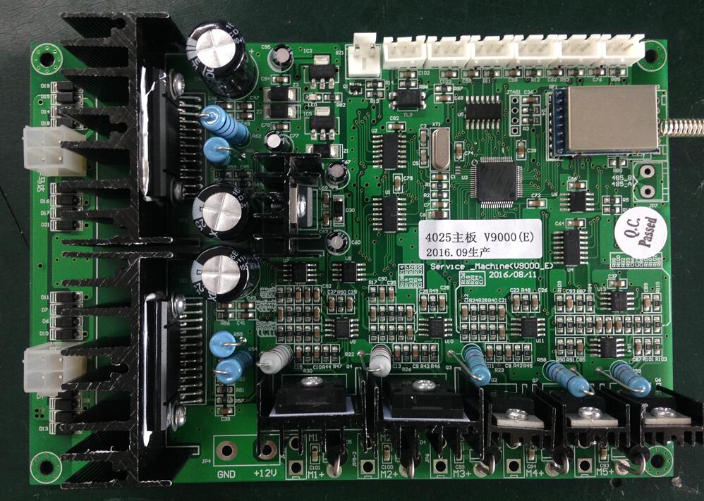
Design and development of Zhongshan electronic control board
The basic process of planning circuit board can be divided into three steps: the planning of circuit schematic diagram, generation network table and PCB planning. Whether it is the layout of the equipment on the board or the routing, etc., there are specific requirements.
The input and output wiring shall be as parallel as possible to avoid interference. It is necessary to add ground wire to block the parallel routing of two signal lines. The two adjacent layers should be perpendicular to each other as much as possible, and the parallel and simple parasitic coupling should occur. The power supply and ground wire shall be divided into two layers as perpendicular to each other as possible. In terms of linewidth, a wide ground wire can be used as a primary circuit for digital circuit PCB, that is, to form a ground network (analog circuit cannot be used in this way), and lay copper on a large area.
Equipment layout
In terms of the layout of the components, the components related to each other should be placed as close as possible. For example, the clock generator, crystal oscillator and the clock input of the CPU are prone to noise, so they should be placed closer. As for the equipment, small current circuit and large current circuit switch circuit which are easy to produce noise, it should be far away from the logic control circuit and memory circuit (ROM and RAM) of single chip microcomputer as far as possible. If possible, these circuits can be made into circuit board additionally, which is conducive to anti-interference and improves the reliability of circuit work.
Zhongshan electronic control board http://www.yunhedianzi.com/
-
05-06
The function of Zhongshan intelligent control board in smart home
As we all know, smart home system can make us enjoy life easily. With the continuous development of people's consumption demand and the intellectualization of houses, smart home system products
-
05-06
How to develop intelligent industrial control board based on industrial Internet of things
Today, technology has entered people's day, our day has changed dramatically. People enjoy the surprises and experience brought by technology, but also have more expectations and requirements fo
-
05-06
Zhongshan intelligent control board analysis in the new trend of industrial Internet of things, intelligent control board performance?
In recent years, technology has been developed in an all-round way, and artificial intelligence has entered the initial stage. 5g, machine algorithm and deep learning are no longer just marketing co
-
05-06
Design and development of Zhongshan electronic control board
The basic process of planning circuit board can be divided into three steps: the planning of circuit schematic diagram, generation network table and PCB planning. Whether it is the layout of the equ